Core Services
核心服務
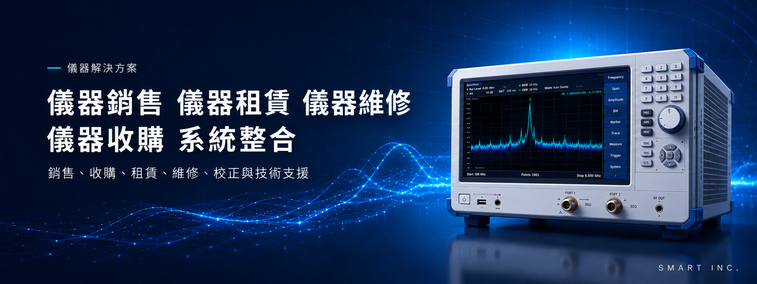
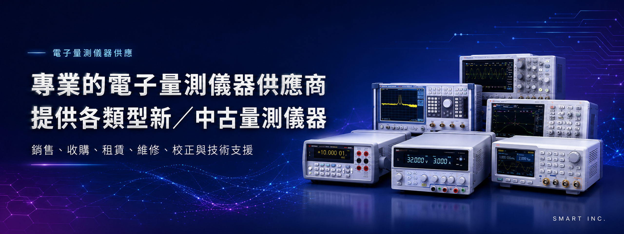
儀器銷售
提供多品牌電子量測儀器與導入建議。
儀器租賃
適合短期專案、驗證測試與彈性需求。
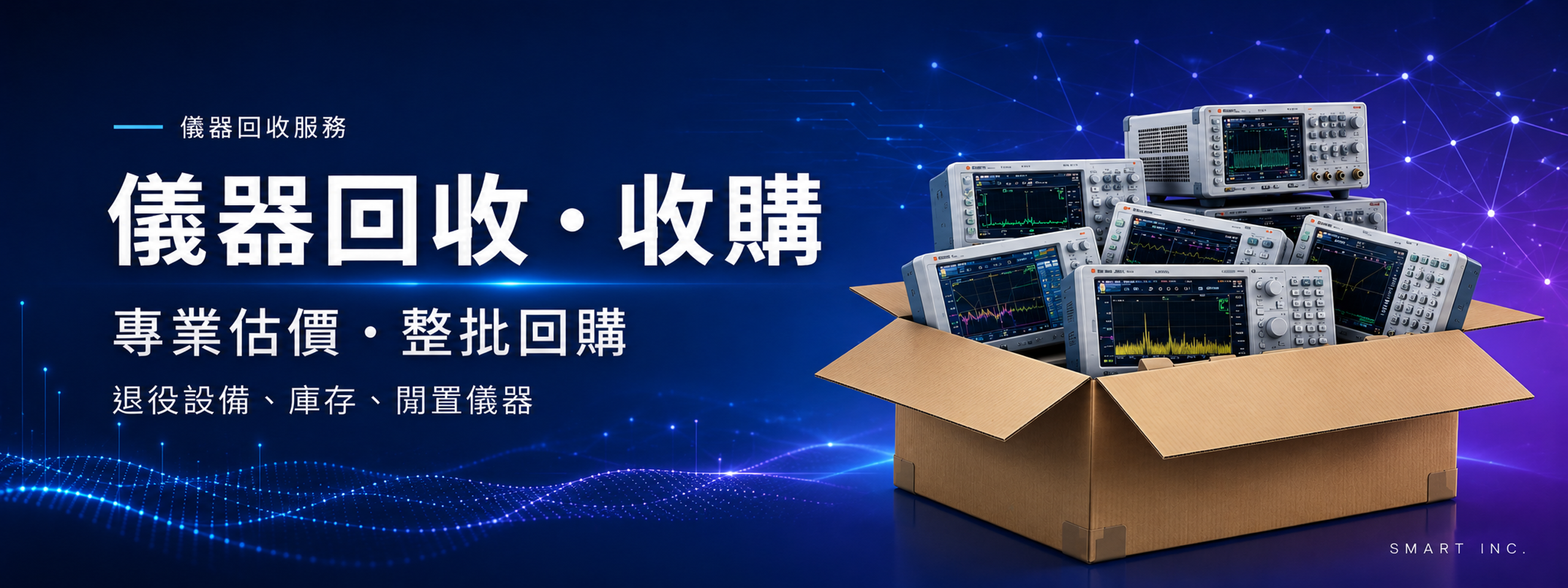
儀器收購
協助退役設備評估與資產再利用。
維修與校正
降低停機風險,維持設備穩定與精度。
Contact Smart Inc.
需要設備建議或技術支援?
歡迎與弘燁科技聯繫,由專業團隊協助您找到更適合的量測解決方案。
AUTHORIZED PARTNER TECHNOLOGY
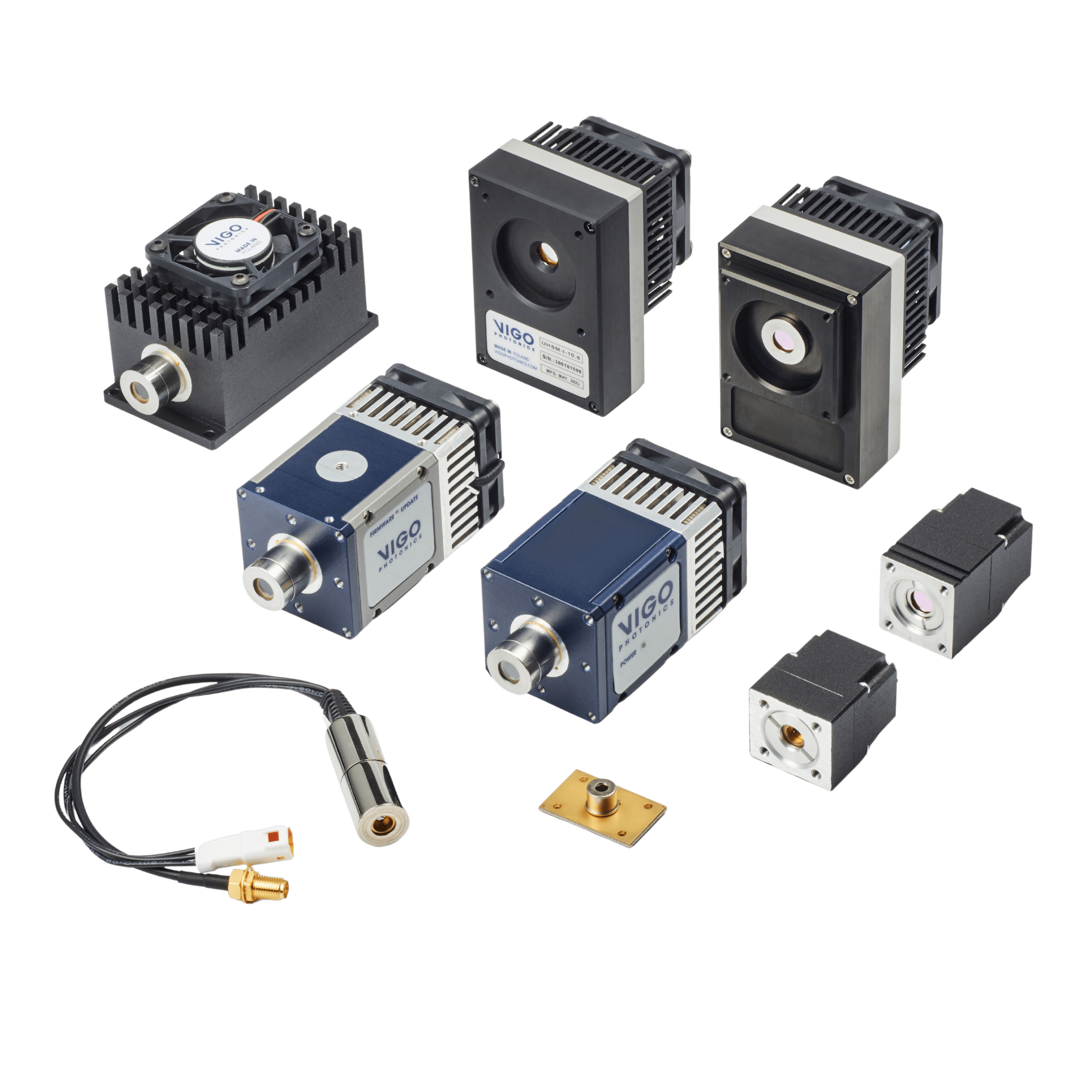
VIGO Photonics 專區
SMART × VIGO PHOTONICS TAIWAN
紅外線偵測器、模組與無人機感測應用支援
SMART 提供 VIGO Photonics 紅外線偵測器、Detection Modules、多通道陣列與 Epi-Wafers 的在地選型、規格確認、datasheet 與技術詢問支援,並協助無人機 / 移動式平台的氣體偵測、環境監測與安全巡檢應用評估。
無人機 / 移動式氣體偵測應用
針對大範圍巡檢、環境監測、管線安全與工業氣體偵測場景,協助評估偵測器、模組與光譜系統整合需求。
針對大範圍巡檢、環境監測、管線安全與工業氣體偵測場景,協助評估偵測器、模組與光譜系統整合需求。